- 您现在的位置:买卖IC网 > Sheet目录344 > MPC8272ADS (Freescale Semiconductor)KIT DEVELOPMENT MPC8272
Hardware Preparation
?
?
?
?
?
?
?
?
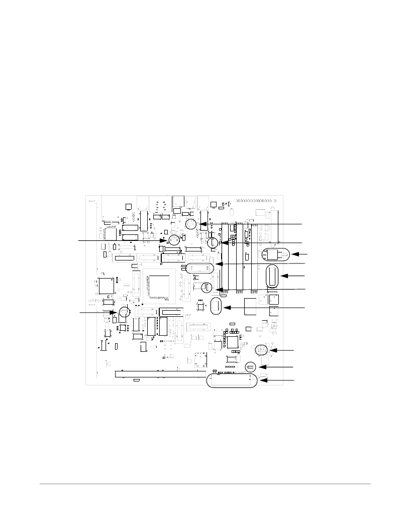
PowerQUICC II’s PCI_DLL using SW2(3)
Clock-in source—external or on-board clock oscillator—JP1
FCC1 and FCC2 MII/RMII modes—using jumpers JP5 and JP10, respectively
USB speed (12Mbits/s or 1.5Mbits/s) software controlled in BCSR
USB host/slave mode—using jumper JP8
PowerQUICC II’s COP/JTAG connection—COP/JTAG connector (P21) or direct
connection to PC parallel port (P27). Selected automatically by connecting parallel
cable.
Force PC parallel port (P27) connection using jumper JP12
ATX power supply on/off switch using SW4
JP8
JP5
JP1
JP10
SW4
P21
SW5
JP9
SW2
RP1
JP12
P27
Figure 2-1. MPC8272ADS Top Side Part Location Diagram
MPC8272ADS User Guide
发布紧急采购,3分钟左右您将得到回复。
相关PDF资料
MPC8308-RDB
BOARD REF DESIGN MPC8308
MPC8309-KIT
KIT EVALUATION FOR MPC830X
MPC8315E-RDB
PROCESSOR BOARD PWRQUICCII PBGA
MPC8349E-MITX-GP
KIT REFERENCE PLATFORM MPC8349E
MPC8349E-MITXE
BOARD REFERENCE FOR MPC8349
MPC8377E-MDS-PB
BOARD MODULAR DEV SYSTEM
MPC8569E-MDS-PB
BOARD MOD DEV SYSTEM MPC8569
MPC8572EAMC
MPC8572 AMC RAPID SYSTEM
相关代理商/技术参数
MPC8272CVR
制造商:MOTOROLA 制造商全称:Motorola, Inc 功能描述:MPC8272 PowerQUICC II Family Hardware Specifications
MPC8272CVRB
制造商:FREESCALE 制造商全称:Freescale Semiconductor, Inc 功能描述:PowerQUICC II⑩ Family Hardware Specifications
MPC8272CVRE
制造商:FREESCALE 制造商全称:Freescale Semiconductor, Inc 功能描述:PowerQUICC II⑩ Family Hardware Specifications
MPC8272CVRI
制造商:FREESCALE 制造商全称:Freescale Semiconductor, Inc 功能描述:PowerQUICC II⑩ Family Hardware Specifications
MPC8272CVRM
制造商:FREESCALE 制造商全称:Freescale Semiconductor, Inc 功能描述:PowerQUICC II⑩ Family Hardware Specifications
MPC8272CVRMIBA
功能描述:微处理器 - MPU 266 MHz 505.4 MIPS
RoHS:否 制造商:Atmel 处理器系列:SAMA5D31 核心:ARM Cortex A5 数据总线宽度:32 bit 最大时钟频率:536 MHz 程序存储器大小:32 KB 数据 RAM 大小:128 KB 接口类型:CAN, Ethernet, LIN, SPI,TWI, UART, USB 工作电源电压:1.8 V to 3.3 V 最大工作温度:+ 85 C 安装风格:SMD/SMT 封装 / 箱体:FBGA-324
MPC8272CVRP
制造商:FREESCALE 制造商全称:Freescale Semiconductor, Inc 功能描述:PowerQUICC II⑩ Family Hardware Specifications
MPC8272CVRPIEA
功能描述:微处理器 - MPU 300 MHz 570 MIPS
RoHS:否 制造商:Atmel 处理器系列:SAMA5D31 核心:ARM Cortex A5 数据总线宽度:32 bit 最大时钟频率:536 MHz 程序存储器大小:32 KB 数据 RAM 大小:128 KB 接口类型:CAN, Ethernet, LIN, SPI,TWI, UART, USB 工作电源电压:1.8 V to 3.3 V 最大工作温度:+ 85 C 安装风格:SMD/SMT 封装 / 箱体:FBGA-324
